Imagine trying to build the world’s most precise machine while standing on a boat rocking in a storm. That is essentially what engineers face when they try to grow perfect semiconductor crystals on Earth. Gravity pulls heavy atoms down, creates turbulent flows in molten materials, and introduces defects that limit chip performance. But what if you could remove gravity from the equation entirely? This is not science fiction anymore. It is the emerging reality of semiconductor manufacturing in space, a field that leverages microgravity processing to produce higher-quality chips and materials than are possible on Earth.
We are entering a new era where Low Earth Orbit (LEO) becomes a factory floor. NASA and private companies are betting big that the unique environment of space-specifically its lack of gravity, ultra-high vacuum, and ability for containerless processing-can solve problems that have plagued terrestrial fabs for decades. If this works, it won’t just mean better phones; it could revolutionize quantum computing, power electronics, and high-performance optics.
Why Earth’s Gravity Is the Enemy of Perfect Chips
To understand why we need to go to space to make better chips, we first have to look at what goes wrong here on Earth. Semiconductor manufacturing relies on growing incredibly pure crystals. Think of these crystals as the foundation of a skyscraper. If the foundation has cracks or uneven layers, the whole building is compromised.
On Earth, gravity drives two main enemies of quality: buoyancy-driven convection and sedimentation. When you melt silicon or compound semiconductors like gallium arsenide, the heat causes fluid movement. Heavier elements sink, lighter ones rise. This creates turbulence and uneven mixing. As the material cools and solidifies, these inconsistencies freeze into the crystal structure as defects, dislocations, or compositional variations.
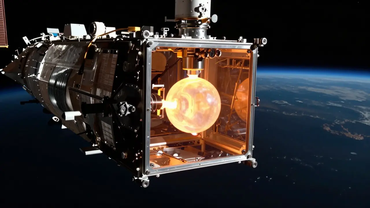
In microgravity, those forces vanish. Without gravity pulling things down or pushing them up, the melt remains still. Dopants (the impurities added intentionally to change electrical properties) stay uniformly distributed. This allows for slower, more controlled solidification. The result? Crystals with far fewer defects and greater uniformity. For advanced applications where even a single defect can ruin a device, this difference is massive.
The Three Pillars of Space Processing
Space offers three distinct environmental advantages that terrestrial labs struggle to replicate without enormous cost and complexity:
- Microgravity: Eliminates buoyancy and sedimentation, allowing for uniform mixing and stress-free crystal growth.
- Ultra-High Vacuum: The natural vacuum of space is cleaner than any chamber on Earth, reducing contamination during sensitive processes like epitaxy.
- Containerless Processing: Materials can be levitated using electromagnetic fields, meaning they never touch a crucible or wall. This prevents impurities from leaching into the melt from the container itself.
These factors combine to enable the creation of metastable phases-crystal structures that are energetically favorable but impossible to form under Earth’s gravitational pressure. These new phases could unlock novel electronic properties currently out of reach.
From Skylab to InSPA: A Brief History
This isn’t a brand-new idea. The roots of space-based materials processing go back to the 1960s and 1970s, with early experiments on Skylab and Soviet missions. During the 1980s and 1990s, Space Shuttle missions carried payloads investigating how weightlessness affected solidification patterns. However, these were largely scientific curiosities rather than industrial plans.
The International Space Station (ISS), permanently crewed since 2000, changed the game. It became a long-duration laboratory where researchers could study optical fibers, specialty alloys, and crystals over months, not days. While much public attention focused on ZBLAN optical fiber production, similar principles applied to semiconductor-grade materials.
In the 2020s, NASA formalized this effort under the banner of In-Space Production Applications (InSPA), a portfolio specifically targeting commercial manufacturing in LEO, including semiconductors, pharmaceuticals, and advanced materials. Simultaneously, academic institutions like Stanford University launched workshops such as “Semiconductor Manufacturing in the Space Domain” to map out technical roadmaps and economic viability. We have moved from asking “Can we do it?” to “How do we scale it?”

Who Is Building Factories in Orbit?
While NASA provides the framework and initial research, private companies are driving the commercial vision. One prominent example is Space Forge, a UK-based company planning to manufacture high-value crystals and semiconductor substrates in space and return them to Earth via dedicated re-entry vehicles. Their model is clever: instead of building a full fab in orbit, they focus on the gravity-sensitive steps-bulk crystal growth-and then ship the resulting ingots back to terrestrial facilities for standard lithography and etching.
This hybrid approach makes economic sense. Launch costs are falling, but they are still significant. You cannot launch tons of sand to make cheap memory chips. But you can launch kilograms of specialized substrate material for quantum sensors or wide-bandgap power devices, where the value per gram is extremely high. Other concepts involve free-flying manufacturing modules that operate autonomously, isolating hazardous high-temperature processes from crewed stations.
Which Processes Benefit Most?
Not every step of semiconductor fabrication needs to move to space. Full-scale integrated circuit assembly will remain on Earth for the foreseeable future due to the complexity and volume required. Instead, specific process classes are targeted for microgravity enhancement:
| Process Type | Benefit in Space | Application |
|---|---|---|
| Bulk Crystal Growth | Reduced convection and thermal gradients lead to fewer dislocations. | Gallium Arsenide, Indium Phosphide substrates |
| Zone Refining | Containerless processing achieves higher purity levels. | High-purity dopant profiles for quantum devices |
| Thin-Film Deposition | Ultra-vacuum reduces contamination; stable gas flows improve homogeneity. | Molecular Beam Epitaxy (MBE), MOCVD |
| Annealing | Uniform heating without buoyancy-induced stress allows precise defect engineering. | Recrystallization of complex oxides |
For instance, growing compound semiconductors like indium phosphide is notoriously difficult on Earth because the components have different densities and tend to separate. In space, they stay mixed, allowing for larger, more homogeneous crystals essential for high-speed telecommunications and laser diodes.

The Economic Reality: High Value, Low Mass
Let’s talk numbers. The biggest hurdle is cost. Even with reusable rockets, launching payload to LEO costs thousands of dollars per kilogram. Returning it safely is even harder. Therefore, space manufacturing must follow a strict rule: high value, low mass.
You won’t see space-made smartphone processors anytime soon. The margin is too thin. Instead, the market lies in niche, high-performance sectors. Quantum computing requires qubits with near-zero defect rates. Power electronics for electric grids need wide-bandgap materials that can handle extreme voltages. Integrated photonics demands glass-semiconductor composites with perfect clarity. These products command premium prices that can absorb the logistics costs.
Analysts compare this to the early days of aerospace manufacturing. Initially, only satellites and military equipment justified the expense. Today, consumer tech benefits indirectly from those advancements. Similarly, space-grown semiconductors may start in specialized labs before trickling down to broader applications if costs continue to drop.
Challenges Beyond Physics
It’s not just about physics. There are significant operational hurdles. Equipment in space must be fully automated and fault-tolerant. You can’t send a technician up to fix a jammed wafer handler. Systems must withstand radiation, thermal cycling, and vibration during launch. Maintenance must be remote.
Then there’s regulation. Semiconductor technology is heavily scrutinized for national security reasons. Export controls dictate who can buy advanced chips and where they can be used. Manufacturing them in international waters-or rather, international orbit-adds a layer of legal complexity. Who owns the intellectual property? Which country’s laws apply? These questions are still being answered by policymakers.
What Comes Next?
The next decade will be defined by experimentation. We need more data. How much does defect density actually drop? Is the improvement statistically significant enough to justify the risk? Stanford’s workshops and NASA’s InSPA initiatives are laying the groundwork, but we need repeated, large-scale demonstrations.
If the data holds up, we could see the first commercial batches of space-grown substrates arriving on Earth by the early 2030s. They won’t replace your local foundry. Instead, they will sit alongside it, providing the premium ingredients for the next generation of technology. The journey from Skylab’s small experiments to orbital factories is long, but the destination-a world where gravity no longer limits our technological potential-is worth the trip.
Will space-manufactured semiconductors replace Earth-based fabs?
No, not in the near term. Space manufacturing focuses on high-value, low-volume steps like bulk crystal growth. The majority of chip fabrication, including lithography and assembly, will remain on Earth due to the massive scale and infrastructure required.
What is InSPA?
In-Space Production Applications (InSPA) is a NASA initiative aimed at fostering commercial manufacturing in Low Earth Orbit. It highlights sectors like semiconductors, pharmaceuticals, and advanced materials that benefit from microgravity.
Why is microgravity better for crystal growth?
Microgravity eliminates buoyancy-driven convection and sedimentation. This prevents heavier elements from sinking and lighter ones from rising, resulting in more uniform mixing and fewer structural defects in the final crystal.
Which companies are involved in space semiconductor manufacturing?
Companies like Space Forge are leading the charge, focusing on growing high-quality crystals in space and returning them to Earth. NASA and academic institutions like Stanford also play key roles in research and policy development.
When will we see commercial products from space fabs?
While experimental payloads are active now, widespread commercial availability of space-grown semiconductor substrates is likely several years away, potentially in the early 2030s, depending on cost reductions and successful validation trials.
14 Responses
gravity is just a suggestion really when you look at the universe on a quantum level we are all floating in a sea of probability and these crystals are just trying to find their true form without the heavy hand of earth pulling them down into mediocrity
another american dream gone wrong spending billions to make chips in space while our domestic infrastructure crumbles under the weight of foreign dependency it is pathetic that we rely on uk companies like space forge for this basic innovation we should be leading not following
bro this is literally scienc fiction come to life i mean sure the costs are insane but imagine having a phone that never lags because the chip was grown in zero g its gonna change everything trust me the hype is real even if my spelling is bad today
the pursuit of perfection in a flawed universe is a noble endeavor yet one must wonder if the defects we seek to eliminate are merely shadows of our own imperfections projected onto the silicon lattice
stop dreaming about space factories and focus on fixing the supply chain here on earth until you can produce reliable semiconductors domestically you have no business talking about orbital manufacturing it is a distraction from real economic issues
i get the excitement but let us keep our feet on the ground or at least acknowledge the massive logistical hurdles we need to support the workers who will maintain these systems remotely safety and reliability must come before profit margins
actually the thermodynamic implications of containerless processing in microgravity are far more significant than most realize the elimination of crucible contamination allows for metastable phases that are theoretically impossible under terrestrial gravitational constraints which fundamentally alters the bandgap engineering possibilities for wide-bandgap semiconductors
they say its for science but really its just another way for big tech to control what we buy and think the government knows exactly how many defects are in your phone they want you to believe space makes it better so you pay more
perhaps the silence of space offers a clarity that noise of earth cannot provide and in that quiet we might finally hear the truth of matter itself
everyone is too busy looking up at the stars to notice the holes in the argument launching materials to orbit is exponentially more expensive than refining them on earth unless you are selling to governments this business model is pure fantasy
it is fascinating to see how different cultures approach this technological leap while some see only cost others see the potential for global collaboration in solving material science challenges we must embrace this diversity of thought to move forward together
while the technical details are impressive we must remain grounded in the reality that human ingenuity has always found ways to overcome physical limitations whether on earth or in space the spirit of innovation remains constant
i truly appreciate the detailed breakdown of how microgravity affects crystal growth because understanding these nuances helps us all feel more connected to the scientific process and reminds us that every small step towards better technology is a victory for humanity as a whole
india has been pioneering satellite technology for decades and understands the value of high precision materials the jargon used here regarding epitaxy and zone refining is accurate but the real question is whether western companies can match the efficiency and cost-effectiveness that asian manufacturers have already achieved in terrestrial fabs